|
|||||||||||||||||||||||||||||||||||||||||||||||||||||||||||||||||||||||||||||||||||||||||||||||||||||||||||||||||||||||
|
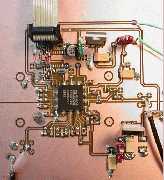
AD9852 DDS experimentation By F6EHJ - Gérard LAGIER (F6EHJ@wanadoo.fr) DDS are not as versatile as they appear and one of the main drawback is the presence of SFDR (Spurious Frequency Dynamic Range) which occur all over the spectrum. These spurious are really difficult to remove, I should say impossible, and the use of a DDS to built a high performance local oscillator is really a nightmare. I tried several DDS (AD9832, AD835, AD9850 and AD9851) from Analog Device, they mainly differ in term of maximum clock frequency. The AD9850 is able to be feed with a 125 MHz clock, the AD9851 with a 180 MHz clock. In fact, both can support 180MHz, the only problem is the heat dissipation. The usual rule in order to know the maximum output frequency is to take 40% of the clock frequency. For instance, with an AD9850 running at 125 MHz, the maximum output frequency will be 50 MHz. Unfortunatly, even at lower frequencies, the output signal is far to be very clean and a lot of unpredictible spurious are present at the output. Using the signal as a local oscillator allows a lot of birdies during frequency scan. One of the way to "clean" the output is to use a combination of a DDS with a VCO and a PLL. This "clean-up" VCO is really effective and I recently built a LO like this. The cleaning process is mainly performs using the DDS at a very low frequency (3 to 5 MHz). The drawback is the need of more than one VCO if we consider to cover the 9 amateur bands. My last experimentation was using 4 VCO for 1.8 to 54 MHz. It works very well but the number of components is impressive and the time spent to tune the board was impressive too !! Few years ago, Analog Device put the AD9852 on the market. This DDS is quite similar to the other (except the maximum voltage which is 3.3V) but the main improvement is the 12 bit DAC resolution (10 bits for the others mentionned before). These 2 bits make really the difference as it can be seen on the data sheet when you go deep inside to the SFDR curves. The main drawback of this DDS is its package....A 80 pin chip....!! I should confess the package was the main problem. Finally, I considered the AD9850 and saw that the space between each pin was the same...! So why not ? Once the decision taken, the data sheet read and read again (obviously not very easy), I started to look on the web for similar experimentation. Searching for "AD9852" or "AD9854" (quite the same), gave me some material back. Unfortunatly, none of the projects described were using my usual interface (PIC Microchip) and mainly were interfaced to the printer port of a PC like the AD experimentation board. The first round was to draw the circuit (I use PROTEUS CAD) and then to make the small PC board. The target was to know if I was able to speak clearly to the chip. Once the PC board was done, I have to mount the two 3.3V low drop regulators (as the data sheet mentionned, it is better to use separate power supply for the digital and the analogic section) and then the chip itself...A great moment according to the pin number...!! In order to do that, I used my usal procedure for the AD9850 : all the pin are soldiered together, the excess amount was then removed. The operation cannot last a while...Try to do that fast. Anyway, it has to be done with calm and cold blood. See the experiment board :
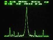
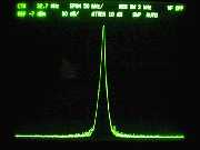
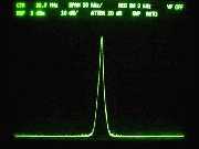
The interface between the DDS and the PIC is a little bit special because the DDS is limited to 3.3V on its pins. The PIC delivers a 5V signal, so an adaptation must be done. The simplest way is to use a resistor divider for each pin, lowering the 5V to 3.3V. Unfortunaltly, I never really succeeded in this way : the DDS was not working all the time. Finally I used the circuit describes by Charlos POTMA (PA3CKR) on his site. It simply uses diodes conected to the 3.3V rail to lower the TTL signal coming from the printer port or the pic. It perfectly works and seems to be very reliable. The next step was to write a very small piece of software for the PIC, in order to command the DDS. After some "cut and try", I finally find out the good configuration to output a beautiful 10 MHz signal from the DDS. Provision were not made on the PC board for the clock oscillator, so I used my HP signal generator to feed the clock input of the AD9852. This allows to test the clock sensivity, moving the frequency down to a couple of MHZ to the upper limit. Before running this test, it is important to know that the AD9852 requires more command lines than the AD9850. The architecture is not the same: a Master Reset is absolutly necessary (I used a hardware reset for the test), an IO Reset is also required and if you want to use an other item which share the data and working lines with the DDS, the Chip Select pin must be activated. DATA and W_CLOCK are the same as the other DDS. The IO Update pin could also be used if necessary, I'd rather use the internal IO Update for the moment. The clock frequency upper limit was reached carefully, taking into account the data sheet recommandations concerning the heat dissipation. Using an AD9852 AST (plastic package), the upper limit is 200 MHz, the ASQ package accepts 300 MHz if properly mounted. At a frequency clock of 200 MHz, the purity of the signal is very good and has no relationship with the output of an AD9850. No one spur on my spectrum analyser can be seen on a 10 MHz signal. At 60 MHz output with the same 200 MHz clock, the spurs start to be visible, but the level remains very low. No big spike as before... The clock was then increased to 250 Mz, then 300 MHz. At this frequency, the chip starts to heat fast (keep your finger on) but tests can be made during 10 seconds without problem. The gain is mainly in the high output frequencies and a clean 120MHz signal is easily obtainable with a 300 MHz clock. The final test was to evaluate the maximum clock frequency. It was found out around 450 MHz for the chip I have. Of course, the heat dissipation is very high (more than 1 amp) and the temperature increases very fast. No more measurement at this frequency have been done due to the temperature. So, dont go over 200 MHz with the AST package. The ASQ can support higher frequency clock (if needed) but requires a dissipator to evacuate the heat. I plan to experiment it latter. If low phase noise is needed, the clock oscillator will have to be design carefully. The use of "packed TTL oscillator" is prohibited and a discrete components oscillator should be preferred. 200 MHz crystal are waited soon for further experiment. The other way is to use the internal multiplier which allows a continuous multiplication factor of 4 to 20.To do that, the PLL must be ON and draws some extra current and produces some heat too... Using a 15 MHz oscillator permits to get a 300 MHz signal clock. However, the multiplier has a clear effect on the spectrum and side band noise appear frankly. More the multiplicator number is high, more the noise and spur. As the DDS itself, the PLL is able to provide a 450 MHz clock to the DDS core. AD9850 versus AD9852 : As mentionned earlier, the difference appears in the upper part of the spectum and the three following pictures show the phenomena. The first picture is an AD9850 with a 80 MHz clock outputing a 32 MHz signal (roughly the AD limitation). The second picture is an AD9852 with the same 80 MHz clock and the same output signal. The third one is an AD9852 clocked at 200 MHz and delivering the 32 MHz signal. Comments are welcomed...!
Following are the schematic of an RF generator project (not already build) using an AD9852 and a PIC 16F877. Gérard LAGIER /F6EHJ DDS SECTION PIC SECTION LCD SECTION Printed Circuit |


